


The FPTA chip is an ASIC, designed in the Electronic Vision(s) group, which is dedicated to Hardware Evolution of analog electronic circuits. The Heidelberg FPTA Hardware Evolution System uses this chip as a substrate on which candidate solutions produced by the Evolutionary Algorithm 'live', that is, their ability to solve the problem at hand is tested by measuring their behaviour when downloaded to the FPTA chip.
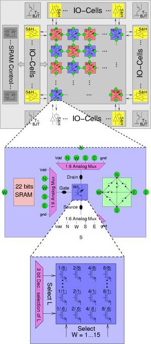
The top of the adjacent figure depicts a schematic overview of the FPTA chip. The core part of the chip consists of an array of 256 programmable transistor cells. As CMOS transistors come in two flavours, namely as P- and NMOS, these are arranged in a checkerboard pattern. This matrix of transistor cell is programmable in the following twofold sense: First, the channel dimension (width and length) of each transistor cell can take on 75 different values and second, the terminals of these transistor cells can in principle be connected freely with each other. However, since the chip is an actual piece of hardware, the routing capabilities are finite. Each of the transistor cells stores its configuration bits in its own SRAM, which can be written to and read from by the SRAM control logic.
The tranistor array is surrounded by 64 input/output (IO) cells. Each of these 64 IO-cells can be configured to feed a signal into the according border cell of the transistor array or to sample its output which can subsequently be converted to a digital signal off-chip. Inputs and outputs are multiplexed to the IO-Cells from one analog in- and one analog output respectively.
The middle of the accompanying schematic drawing shows a close-up of one PMOS-transistor cell. Each of the transistor terminals of the programmable transistor can be multiplexed to any of the four corners of the cell (North, East, South, West) or to either of the power supply voltages vdd / gnd. Please note that the green circles in upper and middle part of the schematic both depict the connections of the transistor cell and that those with the same initial letter of a cardinal point are directly connected with each other. Besides the routing of the transistor terminals, any of the four cell boundaries can be connected to any of the remaining ones by means of the switch matrix drawn in green. Since this - for reasons of symmetry and simplicity - is the only way of signal routing, some of the transistor cells will have to be sacrificed in favor of signal routing.
The process of selecting the desired channel dimensions for the programmable transistor is in fact done by choosing among different transistors. Altogether five different channel lengths and 15 different channel widths are provided. All unused transistors are switched off.
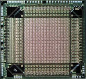
A micro-photograph of the actual die is shown below togehter with a summary of the chip's features.
Features of the FPTA chip:

 HOME
HOME
