


Next: Last but not least
Up: Digital Control Circuitry
Previous: The test pulse circuit
The programming of the Helix128-2's internal registers is achieved via a
simple serial interface of three lines.
In Helix128-2.0/2.1 the three signals involved are SerClk,
SerData, and SerLoad, in Helix128-2.2/2.3
SerClk has been merged with Rclk and SerData
with TrigIn. Thus, in the latter case, programming of
the registers will give rise to multiple triggers; it is therefore
recommended to keep notReset low during programming.
The following explanation applies to Helix128-2.0/2.1, but
is easily extended to the new scheme by making the above
stated substitution.
During programming of the chip Rclk and SerClk must
run continously. A 20 bit word is applied according to the Helix128-2 data
frame (fig. 16) on the SerData line synchronously to
SerClk (fig. 17).
The end of the word is signaled to Helix128-2 by activating
SerLoad; note that SerClk must continue running at least one more cycle.
A Helix128-2 serial data frame consists of the following components:
- The broadcast or common set bit; if set, the chip
address decoding is overridden and the register is set to the
specified value.
- The chip address; the 6 bits of the chip address are
compared to
the signals of the ID<5:0> pads. If they do not match, the
following
bits are ignored (unless the broadcast bit has been set).
- The register address; the 5 bits specify the address of
the
register to be written to.
- The data word; the 8 bits contain the value the specified
register is set
to.
Data are written into the chip with the MSB first.
Tab. 5 shows the map of the register addresses.
Figure 16:
Data format of the Helix128-2 chip
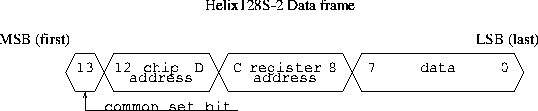 |
Figure 17:
Serial interface timing (Helix128S-2.0/2.1); substituting
SerClk by Rclk and SerData by TrigIn gives the
programming sequence of Helix128S-2.2/2.3.
In the example plotted the Vdcl bias voltage is set to its nominal
(Helix128-2.0/2.1/2.2) value of +1V
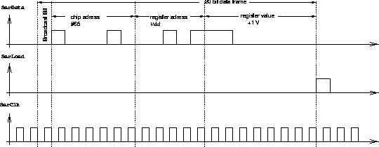 |
Table 5:
Helix128-2 register map
| Register address (HEX) |
(BIN) |
(DEC) |
Register name |
| 01 |
00001 |
01 |
Ipre |
| 02 |
00010 |
02 |
Isha |
| 03 |
00011 |
03 |
Ibuf |
| 04 |
00100 |
04 |
Icomp |
| 05 |
00101 |
05 |
Ipipe |
| 06 |
00110 |
06 |
Isf |
| 07 |
00111 |
07 |
Idriver |
| 08 |
01000 |
08 |
Vfp |
| 09 |
01001 |
09 |
Vfs |
| 0A |
01010 |
10 |
VcompRef |
| 0B |
01011 |
11 |
Vd |
| 0C |
01100 |
12 |
Vdcl |
| 0D |
01101 |
13 |
Voffset |
| 11 |
10001 |
17 |
Latency |
| 12 |
10010 |
18 |
SyncReg |
| 13 |
10011 |
19 |
ClkDiv |
| 14 |
10100 |
20 |
TokenDelay |
Next: Last but not least
Up: Digital Control Circuitry
Previous: The test pulse circuit
Martin Feuerstack
2/3/1999