Next: Digital Control Circuitry Up: Analog Signal Processing Architecture Previous: The current buffer
![]()
![]()
![]()
![]()
Next: Digital Control Circuitry
Up: Analog Signal Processing Architecture
Previous: The current buffer
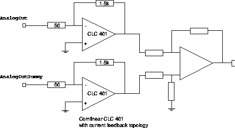
The current signals delivered on AnalogOut and
AnalogOutDummy should be received by a fast (bandwidth 100 MHz)
transimpedance amplifier to make use of the full 40 MHz drive
capability of the onchip current buffer and subtracted from each other
to reduce common mode interference. The schematic depicted in fig.
10 shows the suggested receiver circuit. The
gain delivered at 1.5k![]() transimpedance is
transimpedance is ![]() 85mV/MIP
85mV/MIP![]() (Helix128S-2/2.1) resp. 425mV/MIP
(Helix128S-2/2.1) resp. 425mV/MIP![]() (Helix128S-2.2/2.3). The 50
(Helix128S-2.2/2.3). The 50 ![]() resistors at the inputs were
chosen to terminate properly a 50
resistors at the inputs were
chosen to terminate properly a 50 ![]() cable.
The Comlinear CLC 401 opamp features a high bandwidth
and the ability to handle large voltage gains (voltage gain = 30 in
the suggested configuration).
cable.
The Comlinear CLC 401 opamp features a high bandwidth
and the ability to handle large voltage gains (voltage gain = 30 in
the suggested configuration).
![]()
 |