


CMOS image sensors are designed and built using standard 'Complementary Metal Oxide Semiconductor' (short: CMOS) technology. The availability of basic circuit elements like diodes and transistors in CMOS processes suggests to use the intrinsic photoelectric effect in the depletion zones of the pn-structures for light detection. The development of own image sensors in CMOS technology offers a major advantage compared to commercially available systems (usually based on CCD technology): one can integrate additional electronics next to the optical sensors on the chip. Thus single chip cameras, which can already perform individually adapted signal processing on the chip, can be realized. This is the basic idea of CMOS photoreceptors ('Vision Chips').
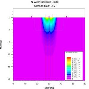
Simulated generation rate of photoelectrons in an n-well/substrate CMOS diode illuminated by a 10 um wide light spot with an intensity of 1 W/m2 at a wavelength of 675 nm. The picture was produced using the 'SILVACO virtual wafer fab' package and is taken from the diploma thesis of Peter Schneider.
Apart from the integration of sensor elements and on-chip signal processing CMOS photoreceptors are characterised by a large dynamic range of 6 orders of magnitude or more. This performance comes close to the human eye and is far better than that of conventional CCD systems. The technical challenge is to convert the initial charge into a useful analog or digital signal. This has to be done on the one hand with respect to signal to noise ratio and achievable dynamic range but on the other hand with respect to the area used by a single pixel. The resulting total pixel size determines the amount of pixels that can be integrated on a given piece of silicon, whereas the so-called fill-factor (ratio of the area of the integrated photodiode to the total area of the pixel) determines the resulting efficiency of the sensor.

 Electronic Vision(s) Group
