


The successful development of new microchips depends not only on inventing and implementing new circuits, but also on the testability of the prototype chips. Each new chip needs an individual test setup to safely power the chip, test its input and output connections and finally verify the complete functionality. Checking the fulfilment of all specifications requires complex digital and analog test patterns as well as the monitoring of the chip response in realtime. The test conditions should be controllable by a PC with the ability to modify the software and hardware environment easily if required.
Besides testing purposes, our group needs fast mixed-signal interface boards to connect evolvable hardware chips (like the FPTA or ANN) to a PC supervising the genetic algorithms. Part of the algorithms should be carried out on the test-board to reduce PCI traffic and CPU utilization. The calculation of an individual's fitness is an example for such a task.
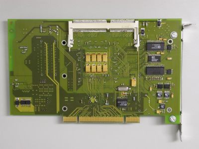
Our group develops PCI-based FPGA boards for these purposes. The current version supports XILINX FPGAs up to the XLA4085 and connects them to the PCI bus via the PLX9054. Fast DAC and ADC channels, together with several bias DACS provide the analog IO. A synchronous static ram supports the FPGA and decouples the pattern generation from the PCI bus. Currently the second generation of FPGA boards is under development, now based on VIRTEX-E FPGAs. Test chips are placed on small carrier boards that can be hot-plugged from the rear of the computer without opening the case. To enhance the flexibility the board supports also a standard CMC card.
The design and test of this board is completed, and it is used in various projects.
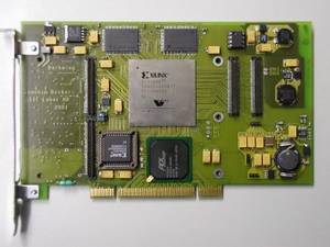
Chipset
Input/Output
Technologies:

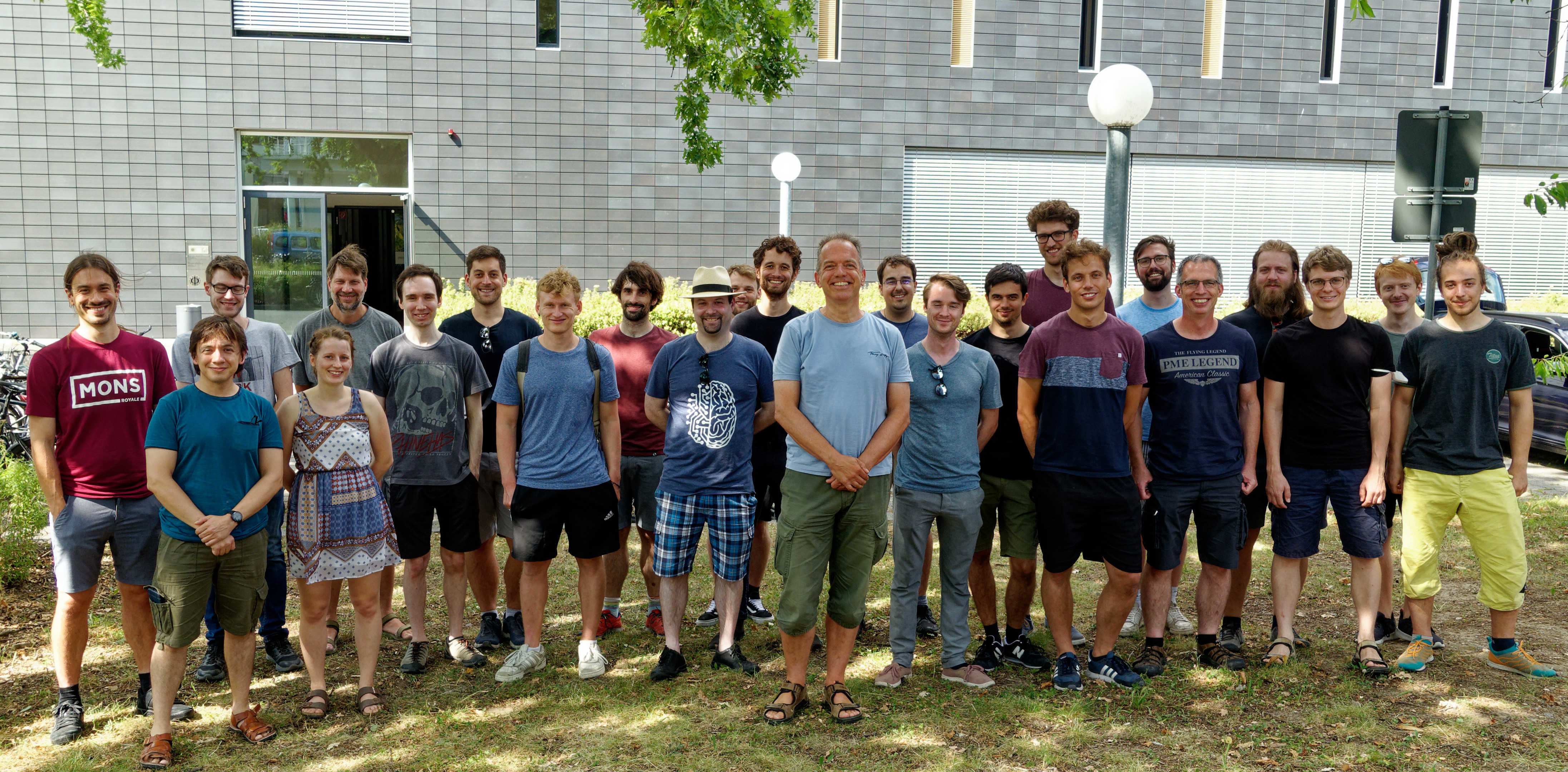
 Electronic Vision(s) Group
